Chemical Vapor Deposition Diamond
Chemical Vapor Deposition diamond (CVD diamond) is a leading edge thermal management material exhibiting thermal conductivities of up to 1800 W/mK, which is five times that of pure copper. Thermal conductivity is the property to conduct heat across a thermal gradient. But it has more unique properties, including optical transparancy and extremely high elastic modulus.
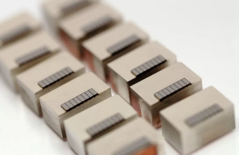
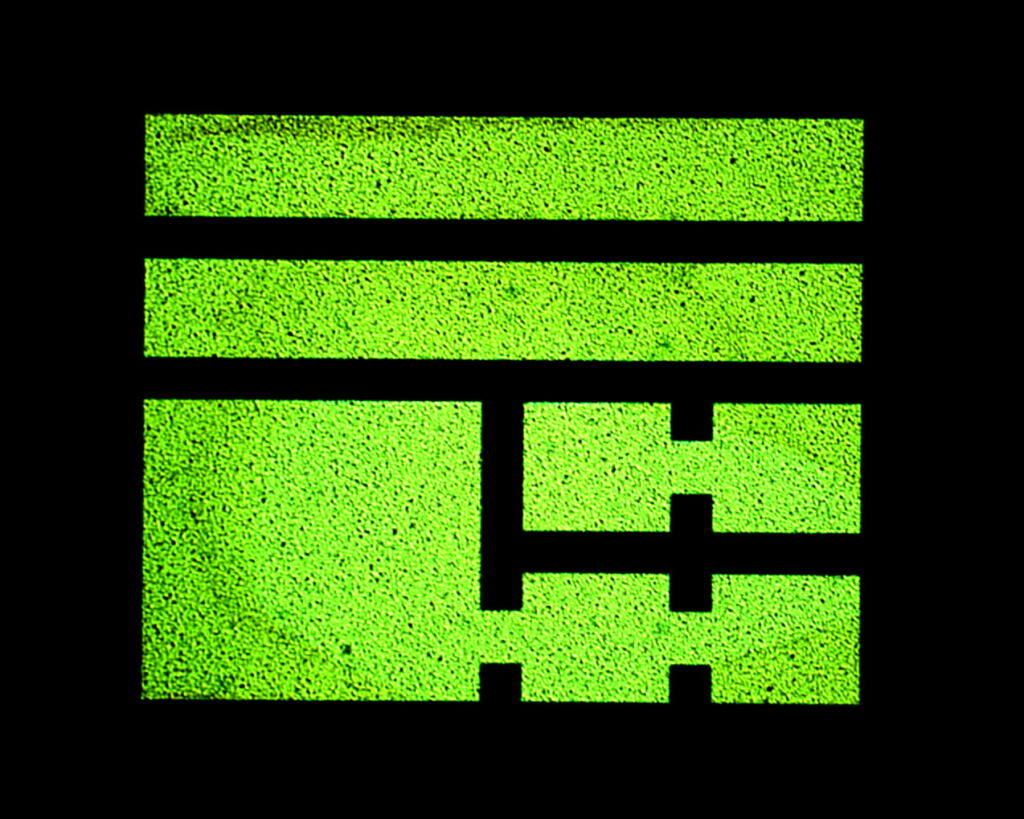
This material is particularly suitable for devices with small heat sources and high power densities such as Laser Diodes (LD), Laser Diode Arrays (LDA) and high power microelectronic devices such as RF amplifiers. As CVD diamond is an electrical insulator, the surfaces can be patterned to form solder mount pads as well as wire bonding areas.
Characteristics of CVD:
- Thermal conductivity (W/mK) (depends on grade): 1000 | 1800
- Coefficient of thermal expansion (ppm/K, @300K): 1.00
- Coefficient of thermal expansion (ppm/K, @1000K): 4.40
- Thermal diffusivity (cm/s) (depends on grade): 5.50 | 10.00
- Density (g/cm3): 3.52
- Young’s Modulus (GPa): 1050
- Specific heat capacity (J/cm3K): 1.90